Combinational Circuits - Design Procedure
Design Procedure of Combinational Circuits
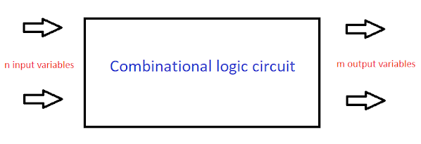
The design of combinational circuits starts from the outline of the problem statement and ends in a logic circuit diagram or a set of Boolean functions from which the logic diagram can be easily obtained.
The design procedure of the combinational circuit involves the following steps :
1. The problem definition.
2. The determination of number of available input variables and required output variables.
3. Assigning letter symbols to input and output variables.
4. The derivation of truth table indicating the relationship between input and output variables.
5. Obtain simplified Boolean expression for each output.
6. Obtain the logic Diagram.
<script data-ad-client="ca-pub-6336795697425578" async src="https://pagead2.googlesyndication.com/pagead/js/adsbygoogle.js"></script>


No comments